Continuing the Ultranet adventure by building a fully functional 8-channel stagebox.
This is a continuation of an already stupidly long adventure; you can read part 1 here but you'll probably need some time to really read it. If you are here just for the demo of the end product, you can click here!
Welcome back!
In the last article, I heavily focused on understanding/reverse-engineering Ultranet and getting a proof of concept working on FPGA. It was mostly about the protocol side: understanding the physical side, how data flows, timings, and wrestling with bits until both transmitter and receiver behaved correctly. As we'll see later, it turns out that I was wrong about the implementation!
In this article, I'm shifting gears to design a product that I'd actually use in live production.
The whole point of this project is to create an 8-channel stagebox for non-critical auxiliary audio lines that I will use in my live production. I recently received the dates and song list for the 2026 "tour" so timelines on multiple projects, including this one, got very real 🤩!
As discussed in part 1, there are many options on the market (ADAT, MADI, Dante, …), but those are (mostly) locked down and expensive. Reusing an existing protocol (like Behringer's Ultranet) is an easy way to design a futureproof(-ish) system while ensuring compatibility with many existing devices, all while learning about the intricacies of the system. This makes me more aware of the limits of a setup and lets me understand why things go wrong and how to bodge said things when it breaks 1h before go-time 😢.
Due to various reasons, I will stop referring to my project as Ultranet. As it is based on AES3, which is an open standard, I doubt I will annoy Behringer too much by publishing this project under a different name. 😅 Therefore, please welcome to the stage: HyperNet 🥁
At the end of part 1, everything was technically working, but not exactly production-ready:
As a reminder, AES3 is designed primarily to support stereo PCM 📊 audio encoded using biphase mark code (BMC).
Biphase mark code, also known as differential Manchester encoding, is a method to transmit data in which the data 💾 and clock 🕓 signals are combined to form a single two-level self-synchronizing data stream.
AES3 is composed of what are called audio blocks. These audio blocks are composed of 192 frames, each frame contains 2 subframes, which, in turn, contain 32 time slots.

A subframe is composed of:
| Time slot | Name | Description |
|---|---|---|
| 0–3 | Preamble | A synchronization preamble |
| 4–7 | Auxiliary sample | A low-quality auxiliary channel used as specified in the channel status word. |
| 8–27 | Audio sample | Audio sample stored MSB last. It can be extended to use the auxiliary sample to increase quality |
| 28 | Validity (V) | Unset if the audio data is correct and suitable for D/A conversion. |
| 29 | User data (U) | Forms a serial data stream for each channel. |
| 30 | Channel status (C) | Bits from each subframe of an audio block are collated, giving a 192-bit channel status word. |
| 31 | Parity (P) | Even parity bit for detection of errors in data transmission. Excludes preamble; bits 4–31 need an even number of ones. |

The preamble can be one of three values:
| Name | Timeslot (Last was 0) | Timeslot (Last was 1) | Function |
|---|---|---|---|
| Z or B | 11101000 | 00010111 | Marks a word for channel A (left), and the start of an audio block |
| X or M | 11100010 | 00011101 | Marks a word for channel A (left) |
| Y or W | 11100100 | 00011011 | Marks a word for channel B (right) |
Between the AES3 and S/PDIF standards, the contents of the 192-bit channel status word differ significantly, although they mutually agree that the first channel status bit distinguishes between the two 🤝. In the case of AES3, the standard describes, in detail, the function of each bit.
Broadly speaking, the channel status word indicates the type of data and has information about the clock and various metadata such as channel origin/destination.
The initial assumption that Ultranet squishes 🗜️ eight 48 kHz audio channels into a single 192 kHz AES3 stream turned out to be correct. In other words, the eight channels are interleaved into one high-rate AES3-like stream so that each 48 kHz channel fits into the 192 kHz timing without resampling.
However, initially, I assumed that Ultranet relied on the AES3 B-frame for channel synchronization, which seemed like a good idea since the protocol is based on AES3 🤔. That assumption was partly correct; it allowed me to receive audio, but it failed when it came to consistent channel indexing while receiving. At the same time, the transmitter either produced misaligned channels or didn't work whatsoever. This meant that the actual synchronization mechanism had to be different 🤨.
This is when Christian Nöding contacted me again. He was working on the Ultranet output of the X32 for the OpenX32 project. I promptly sent him my code to try!
He tested it on a P16-M, and all he got was garbage 🗑️, random noise instead of usable audio. That immediately caught my attention. If his implementation didn't work on an actual Behringer device, something was clearly wrong in our understanding of the protocol.
By pure luck 🍀, I stumbled across a used P16-M listed for almost nothing on my local marketplace, so I grabbed it as soon as I could. Once it arrived, I hooked it up to my setup (the same one that worked flawlessly with the TFX122M-AN) and got the same garbage output. That was both good and bad news. On one hand it meant my implementation wasn't truly compatible, but on the other hand, now, I could reproduce the problem on real hardware and dig deeper into what was actually going on.
I then spent quite a while trying to debug things. At some point I got close and got channels 1-2 working, but after 2 days on the problem I had enough and decided that I wasn't going to test things blindly anymore 👀.
After a break, I promptly started to disassemble the mixer. At first glance/probe, I was surprised that none of the AK4114 appeared to have their B-frame pins connected to the XMOS chip 🤔. This is what set off alarm bells. I promptly soldered jumper wires on the SPI bus used to configure the chips and was again surprised by how little communication there was:

After a quick read of the datasheet, it turns out that their config is very standard. The config sent to the chips is setting one of them to use the crystal as a clock source and the other one as a slave. The config also re-routes their input directly to the output pin for the passthrough port.
I then snooped on the I2S output and B-frame output, which looked like what you would expect. I was so determined to find something weird that I went as far as managing to rebuild a WAV file from a 20-second capture done with the logic analyzer, which also worked just fine 🔊.
Reluctantly, I decided that I might learn something by desoldering the chips 🔥. This confirmed that the only thing connected to the XMOS chip was the I2S signal and the "valid" output. This effectively confirmed that synchronization was in no way tied to the B-frame, and as the channel and user bits weren't connected either, it left only one place where the XMOS chip could sync: the sample data
Now, a sync signal in the sample data sounds wrong. How the hell did they fit 24-bit audio + sync into 24 time-slots 🤨 ????
After some google-fu, it turns out that they don't. Ultranet doesn't use 24-bit PCM, instead it uses 22-bit PCM.
In hindsight, I should have noticed it earlier; most quick start guides from Behringer mention that their A/D conversion is 24-bit, but they do not mention anything about the actual data.
However the guide of some devices (like the DL32) has an interesting line:
ULTRANET networking @ 48 or 44.1 kHz, 22-bit PCM
At the time I thought that was a typo 🤦, but I now realize that it is indeed correct. While the P16-M (and other devices that receive Ultranet) probably use 24 bits for their internal signal processing and the digital-to-analog conversion, the actual digital data transmitted over Ultranet is only 22-bit.
So, what is in those two bits? A bit more digging later, I found a few things on the web:
All of these projects implement some sort of sync based on the sample data 🤯.
Ok, enough teasing. As I said before, since the data itself was correct and I was just receiving channels with an offset, it meant that the block structure was already correct since:

Channel 1 (read subframe 1) being the first in each frame is an editorial choice for this article; the position of the subframe in the frame is not relevant for Ultranet
The subframe, however, is a bit different:

| Time slot | Name | Description |
|---|---|---|
| 0–3 | Preamble | Synchronization preamble, same as AES3 |
| 4–5 | Channel index | Index of a "left/right" channel pair |
| 6–27 | Audio sample | Audio sample stored MSB last. |
| 28 | Validity (V) | Set if the audio data is correct and suitable for D/A conversion. |
| 29 | User data (U) | Unused, set to 0. |
| 30 | Channel status (C) | Used, but structure is currently unknown |
| 31 | Parity (P) | Even parity bit for detection of errors in data transmission. Excludes preamble; bits 4–31 need an even number of ones. |
As you can see, it's stupidly simple, and after a quick analysis with the logic analyzer, here are the channel indices:
| Channel | Index |
|---|---|
| 1 | 00 - Left |
| 2 | 00 - Right |
| 3 | 01 - Left |
| 4 | 01 - Right |
| 5 | 10 - Left |
| 6 | 10 - Right |
| 7 | 11 - Left |
| 8 | 11 - Right |
The choice of two bits is interesting; they could have used a third bit but instead chose to group them by two. That grouping explains why the channels offset always moved two at the same time 🙄.
I also find it very intriguing that the TFX122M-AN worked at all last time 🤔. It must use a different sync "procedure" than the P16-M 🤷♂️.
This is superb news 🥳 because while we lose some fidelity, the implementation just became WAY easier than using the B-frame signal:
What's funny is that the channel status bits are still sometimes needed. I still have no idea what they mean, but for some reason it doesn't always work without them. Since they are not used anywhere, I guess that it's a simple pattern that is enough for the AK4114 to start decoding 🤷.
Now that I've set the record straight, let's actually start with part 2. After wrestling with the implementation, it's now time to clean up the move beyond the code spaghetti. This round of changes is all about making the design more robust, modular, and rack-friendly. In short: less "prototype held together with hopes and prayers", and more "something I can trust".
When I did my last PCB order, I snuck in a devboard for the DIX9211, a 216-kHz Digital Audio Interface Transceiver. This chip is similar to the AK4114 that's being used for almost every Ultranet product I've seen so far. It's partly used to replace the PLL1707 👋. It was responsible for generating the 24.576 MHz system clock that the FPGA used to decode and generate the AES3 data streams.
I'll talk about it later, but this chip also replaces the AES3 receiver inside the FPGA, which simplifies a bunch of things.
Also new, are modular DAC and ADC boards with proper analog frontends. This ensures flexibility, upgradability and reparability within the system. Imagine having to rebuild the whole board because someone blew up an input 🤦
In addition, I'm introducing an RP2040 as a supervisor MCU. It will be used to set up everything to its proper state and interface between the FPGA and other components. At its core, this project is an 8-in 8-out signal processor with interconnects, so it could be used for much more than a digital snake!
A much-needed improvement is a proper 1U case and CAD models to fit everything properly (okay, okay, you got me, a shelf with 3D-printed faceplates, I promise it looks good and feels solid 😉, you'll see!).
The last thing I need to mention is the move from fully open-source implementations to using built-in IPs inside my FPGA. Specifically, the transmitter is now using the Gowin SPDIF TX IP. While I do believe that a fully open implementation would be preferable. I also believe that using the best tools for the job is the smarter choice. I'm still very novice in the FPGA world, and while I could probably fix the previous implementation to make it do what I want, for me, it was just "easier" to use something that already works. Moreover, while this IP is proprietary, it is free, so… 🤷
For the outputs, I decided to stick with the same DAC chip as in the prototype. It performed pretty well for my application and integrated nicely with the FPGA 👍. The big change is moving from single-ended outputs to a fully balanced design. That means cleaner audio, lower noise, and better compatibility with professional gear, especially when running long cables on stage or in a studio.
With the move to balanced audio, it also meant new connectors 🔌. While I've seen balanced audio on TRS jacks before (in fact, my sound card, the UA25EX, does it this way), the proper connector to use is the XLR connector, which is way bigger than the small 3.5 mm jack I was using before.
The PCM5100A part of the schematic is super standard; it's basically a copy-paste 📋 of the datasheet. It's just configured for left-justified operation (via solder jumpers). Unfortunately, the PCM5100A is not a DAC with balanced outputs, so I need to adapt it somehow. The go-to, place & forget IC for this is the DRV134 or the DRV135. These chips are wonderful, but they also cost 5 EUR apiece in low quantities; that would mean 80 EUR of line drivers for the whole system 🤑. Much too expensive!
Instead, I chose to do a bit more work and use the NE5532. Here is how it looks:

So let's break it down. The NE5532 is composed of two independent operational amplifiers:
It then goes to protection resistors and DC-blocking caps and finally ends up in the connector 🔌. The same frontend is repeated for the 2nd channel
The PCB itself is basic, although I took special care while routing the analog and digital parts to ensure that they didn't cross. The two ground planes are connected at one point under the PCM5100A as specified in the datasheet.
I also set a specific size limit to the PCB so that I could start 3D modeling 📐 as soon as possible:

The input side follows the same philosophy 🎓: keep the same ADC chip, but redesign the analog front-end for balanced operation. As said before, balanced inputs are essential to reject interference and ground noise. Since XLR inputs are used, the next "logical" step was adding phantom power. While the new board doesn't feature any configurable pre-amplifier (you could technically change the gain of the amp) to boost microphones and whatnot, I figured that adding phantom power couldn't hurt.
If I don't need it, I can simply disable it, but if I want to use microphones, I can simply use inline pre-amplifiers like the Klark Teknik Mic Booster CT1, which is a compact dynamic microphone booster with high-quality preamps. Super easy and pretty cheap!
It does add some complexity (especially since this modification came later, which meant the PCB had to stay the same size to avoid redesigning CAD models), extra power regulation, and proper protection circuits, but it opens up much more flexible use cases. Here is how one channel looks:

As you might have guessed, there's also a go-to IC for this application, the INA137. But same as before, this chip is far too expensive 💸 (less so but still). Instead I choose to use the OPA1677.
But first, we need to talk about what the hell phantom power is 👻. Phantom power is the standard way of powering devices through the same XLR cable that carries the audio signal. Instead of running a separate power line, 48V is applied equally to pins 2 and 3 of a balanced input relative to pin 1. Because the voltage is identical on both pins, it doesn't disturb the differential audio signal. Fortunately, there are plenty of places online to get the technical specifications (IEC 61938:2018 being the official document). Basically the max current is 10 mA, and you only need to connect two 6.81k resistors between each signal pin and the power source. On the schematic, this is the job of R22 and R24. If you would like to learn more about phantom, I can recommend this page: https://sound-au.com/articles/p-48.htm
Note that the specification says 6.81k, but I instead used 6.8k. This is because, apparently, at the time, getting 6.8k resistors with a low tolerance was complicated 🤷. By choosing 6.81k, the specifications ensured the proper tolerance. However, these days it isn't really a problem anymore.
Just after this is the protection circuit; first the signal goes through DC-blocking caps, followed by protection resistors and protection diodes. This circuit ensures that the signal will never have a voltage so far from the absolute maximum that it's going to break something. You'll notice that they are marked as DNP 🤔. It turns out they clamped the signal too much, so I just removed them, and I'll be careful about what I plug in. If you have suggestions, please let me know!
The signal is then biased to 2.5V and fed to an OPA1677 configured as a simple buffer, after which the signal goes through some passives and then goes to the PCM1808!
As before, the PCB itself is basic, and I also took care while routing the analog and digital parts. As with the DAC, the two ground planes are connected at one point under the PCM1808, as hinted in the datasheet.
I also reused the size limit of the PCB that I defined before.

The mainboard changed a lot; in fact, it changed twice while I started the writing process for this article:

As you might be able to see, the SFP and Ultranet ports on the board are basically unchanged. They don't really need to change as they worked perfectly on the prototype. Only the Ultranet TX and RX ports are swapped to facilitate routing and that's it!
This also applies to the FPGA, which is still the same Tang 9k that I used last time. It works very well and is easy to use, so why change it 🙂!
The whole right side of the board is dedicated to power management (3.3v digital, 5v analog, and 48v phantom) ⚡. Each input has its own switch to turn on phantom power instead of a global one.
The most significant change is the IDC ports to connect the ADCs and DACs boards. I chose IDC connectors mainly because they are very resilient, cheap, and widely used. That said, if I were to redesign everything, I would probably use FFC connectors to reduce the size 📏. These ports provide:
Here is a high-level view of the schematic that shows how everything connects to each other:

The last thing that needs a special mention is the DIX9211. This chip is basically an AES3/SPDIF receiver that spits out I2S. This simplifies so much of the FPGA logic since receiving I2S is way easier than receiving AES3!
I'm configuring it with a Raspberry Pi Pico and a few DIP-switches. I also stole the pass-through idea from the P16-M and used the chip as a "biphase router" of sorts. I can configure what input port is used as the input for the DIR, and I can also choose which input port is used for the biphase output. This offers a lot of flexibility; for example, I could use my project to receive from the Ultranet port and at the same time send audio over the fiber link!
This chip was really a no-brainer compared to the PLL1707 that I used before, since for a few cents more, it adds easier decoding, biphase routing, clocks, etc. Massive boost in flexibility for the system!
Here is a diagram showing how the receiver works from a high-level view:

Since the DIX9211 outputs I2S it's pretty simple. The demuxer is the interesting part 🧐. You can find parts of the code below. In short, it loads bits from sdata on the bclk rising edge and saves the sample when lrclk transitions, saving the sample. When two successive samples have the same LSB, output them to their respective ports.
There's a bit of clock management to get the proper speeds for the four I2S outputs and a "small" block to make sure the I2S clocks are somewhat locked to the receiver (which makes sure the samples aren't loaded when written), but that's it.
After that, the signals go to an I2S transmitter block that has been modified to deal with four outputs at once.
 1-- Detect LR transition (channel boundary)
 2is_lr_changed  <= '1' when zlrclk /= lrclk else '0';
 3
 4-- Extract active part of the audio signal and the current LSB of said signal.
 5-- The sample_data signal is 32bit but only the upper 24 bits matter
 6sample_audio_data <= sample_data(31 downto 10) & "00"; -- Remove the LSB as this is used for the channel index
 7sample_lsb_data <= sample_data(9 downto 8);
 8
 9-- Main deserialization process
10deserialize_i2s : process(bclk) begin
11	if rising_edge(bclk) then
12        if reset_n = '0' then
13            -- Reset all outputs and counters
14            sample_data            <= (others => '0');
15            prev_sample_audio_data <= (others => '0');
16            prev_sample_lsb_data   <= (others => '0');
17            ch1_out <= (others => '0');
18            ch2_out <= (others => '0');
19            ch3_out <= (others => '0');
20            ch4_out <= (others => '0');
21            ch5_out <= (others => '0');
22            ch6_out <= (others => '0');
23            ch7_out <= (others => '0');
24            ch8_out <= (others => '0');
25            data_ready <= '0';
26
27            -- Keep the edge detector running while in reset
28            zlrclk <= lrclk;
29        else
30            -- Shift serial input data into buffer (MSB first). 32 bits are shifted but only the upper 24 are valid data
31            sample_data <= sample_data(sample_data'high-1 downto sample_data'low) & sdata;
32
33            -- Save LRCLK for edge detection
34            zlrclk <= lrclk;
35
36            -- On word clock transition:
37            if is_lr_changed then
38
39                -- Check if current LSB matches previous LSB
40                if sample_lsb_data = prev_sample_lsb_data then
41                    -- Two successive samples with same LSB whe are successfuly synced - output them
42                    case sample_lsb_data is
43                        when "00" =>
44                            ch1_out <= prev_sample_audio_data;
45                            ch2_out <= sample_audio_data;
46                        when "01" =>
47                            ch3_out <= prev_sample_audio_data;
48                            ch4_out <= sample_audio_data;
49                        when "10" =>
50                            ch5_out <= prev_sample_audio_data;
51                            ch6_out <= sample_audio_data;
52                        when "11" =>
53                            ch7_out <= prev_sample_audio_data;
54                            ch8_out <= sample_audio_data;
55
56                            -- When channel 8 is written, flag that the data is ready for 1 bclk cycle
57                            -- The choice of lsb=11 is arbitrary, unless the input data is really fucked-up it shouldn't matter. There really should be a separate data ready signal for each pair
58                            data_ready <= '1';
59                    end case;
60                end if;
61
62                -- Store sample and LSB as previous for next comparison
63                prev_sample_audio_data <= sample_audio_data;
64                prev_sample_lsb_data   <= sample_lsb_data;
65
66            else
67                -- Still reading data
68                -- Clear the data ready flag
69                data_ready <= '0';
70            end if;
71        end if;
72	end if;
73end process;
Here is a diagram showing how the transmitter works from a high-level view:

As you can see, it's WAY more complicated than the receiver. This is mainly because I'm using a pre-made FIFO and S/PDIF transmitter block, there's not much code to show besides the diagram, but the most "interesting" part is the mux that pushes a burst of eight audio samples to the FIFO. Basically it waits for the signal that says that the FIFO is almost empty (e.g., finished with the last batch) and pushes the samples.
As before, there's a bit of logic to deal with the clock signals and their synchronization to the transmitter, but that part is pretty easy.
There's also a block to deal with the channel status. I don't really know why it's needed, but I simply use what the DL16 is sending.
 1push_data : process(clk) begin
 2	if falling_edge(clk) then
 3		if reset_n = '0' then
 4            -- Reset all outputs and counters
 5            burst_write_counter <= 0;
 6            sample_write <= '0';
 7            sample <= "000000000000000000000000";
 8        else
 9            -- Data from the I2S reader is ready, burst write the data to the FIFO
10            if data_ready = '1' then
11                burst_write_counter <= 8;
12            end if;
13
14            -- Write samples on a bclk pos edge
15            if bclk_pos_edge = '1' then
16                if burst_write_counter = 8 then
17                    sample <= ch1_in(23 downto 2) & "00";
18                elsif burst_write_counter = 7 then
19                    sample <= ch2_in(23 downto 2) & "00";
20                elsif burst_write_counter = 6 then
21                    sample <= ch3_in(23 downto 2) & "01";
22                elsif burst_write_counter = 5 then
23                    sample <= ch4_in(23 downto 2) & "01";
24                elsif burst_write_counter = 4 then
25                    sample <= ch5_in(23 downto 2) & "10";
26                elsif burst_write_counter = 3 then
27                    sample <= ch6_in(23 downto 2) & "10";
28                elsif burst_write_counter = 2 then
29                    sample <= ch7_in(23 downto 2) & "11";
30                elsif burst_write_counter = 1 then
31                    sample <= ch8_in(23 downto 2) & "11";
32                end if;
33
34                if burst_write_counter > 0 then
35                    sample_write <= '1';
36                    burst_write_counter <= burst_write_counter - 1;
37                end if;
38            elsif bclk_neg_edge = '1' then
39                sample_write <= '0';
40            end if;
41		end if;
42	end if;
43end process;
Since I chose to go with the DIX9211, I need a way to control it 🎛️. This could have been done in the FPGA, however, I didn't feel like implementing I2C by hand 🥱, so I decided to use a Raspberry Pi Pico. It takes up a bunch of space on the PCB, but it's way faster to work with.
Right now it's only configuring the chip, but as I said earlier, I did connect an SPI bus with two extra pins to the FPGA, this could be used for many applications ranging from basic config to audio input/output over USB.
I also alluded to earlier that, like the P16-M, I use the DIX9211 as a router 🔀. This is configured by the supervisor from some DIP switches:
| Config | Behavior |
|---|---|
| xx00 | The output HyperNet signal is coming from fiber input |
| xx01 | The output HyperNet signal is coming from the Ultranet 1-8 input. |
| xx10 | The output HyperNet signal is coming from the Ultranet 9-16 input. |
| xx11 | The output HyperNet signal is coming from the FPGA |
| ------------- | ------------------------------------------------------- |
| 00xx | The DIR input is coming from fiber input |
| 01xx | The DIR input is coming from the Ultranet 1-8 input. |
| 10xx | The DIR input is coming from the Ultranet 9-16 input. |
| 11xx | The DIR input is coming from the FPGA (loopback) |
There are a few additional registers to configure. The full config can be seen in the setup script below.
Again, I didn't feel like setting up a full C++ project with the pico-sdk (or even Arduino), so I just left CircuitPython and made it so that the script runs at boot. This has the downside of a small 500ms delay before it's configured after reset, but I can live with that 🤷!
It could be improved by periodically watching the inputs 👀 and reconfiguring accordingly. It would remove the need to push the reset button after changing the config, but then again, I was lazy for this part of the project.
 1import board
 2import busio
 3import digitalio
 4import time
 5from adafruit_bus_device.i2c_device import I2CDevice
 6
 7source_map = ["Fiber", "HyperNet 1-8", "HyperNet 9-16", "FPGA"]
 8
 9i2c = busio.I2C(sda=board.GP12, scl=board.GP13)
10
11device_dix = I2CDevice(i2c, 64)
12
13def read(device, register, size=1):
14    buf = bytearray(size)
15    with device_dix:
16        device_dix.write_then_readinto(bytes([register]), buf)
17    return buf
18
19def write(device, register, data):
20    buf = bytearray(1)
21    buf[0] = register
22    buf.extend(data)
23    with device_dix:
24        device_dix.write(buf)
25
26config_outsrc_1 = digitalio.DigitalInOut(board.GP0)
27config_outsrc_1.direction = digitalio.Direction.INPUT
28config_outsrc_2 = digitalio.DigitalInOut(board.GP1)
29config_outsrc_2.direction = digitalio.Direction.INPUT
30config_inpsrc_1 = digitalio.DigitalInOut(board.GP2)
31config_inpsrc_1.direction = digitalio.Direction.INPUT
32config_inpsrc_2 = digitalio.DigitalInOut(board.GP3)
33config_inpsrc_2.direction = digitalio.Direction.INPUT
34
35config_outsrc = (not config_outsrc_1.value) << 0 | (not config_outsrc_2.value) << 1
36config_inpsrc = (not config_inpsrc_1.value) << 0 | (not config_inpsrc_2.value) << 1
37
38print(f"DIR Input source: {source_map[config_inpsrc]}")
39print(f"DIR Output source: {source_map[config_outsrc]}")
40
41
42write(device_dix, 0x2F, [0b00000101])    # DIR Output Data Format
43                                         #   24-bit MSB first, left-justified
44
45write(device_dix, 0x31, [0b00000000])    # XTI Source, Clock (SCK/BCK/LRCK) Frequency Setting
46                                         #   SCK=24.576M BCK=12.288M LRCK=192k
47
48write(device_dix, 0x34, [config_inpsrc]) # DIR Input Biphase Source Select, Coax Amplifier Control
49                                         #   rxin0amp normal / rxin1amp normal / rxin2 source
50
51write(device_dix, 0x6F, [0b00011100])    # MPIO_A, MPIO_B, MPIO_C Group Function Assign
52                                         #   MPIO_A = Biphase Input Extension (RXIN8 to RXIN11)
53                                         #   MPIO_B = DIR Flags Output or GPIO (Selected by MPB3SEL, MPB2SEL, MPB1SEL, MPB0SEL)
54                                         #   MPIO_C = DIR BCUV OUT, BFRAME/VOUT/UOUT/COUT
55
56write(device_dix, 0x71, [0b00000000])    # MPIO_B, MPIO_C Flags or GPIO Assign Setting
57                                         #   DIR Flags, set by MPB1FLG / MPC0FLG
58
59write(device_dix, 0x74, [0b01010101])    # MPIO_B1, MPIO_B0 Output Flag Select
60                                         #   LOCK LOCK
61write(device_dix, 0x75, [0b01010101])    # MPIO_B3, MPIO_B2 Output Flag Select
62                                         #   LOCK LOCK
63
64
65write(device_dix, 0x78, [0b11001110])    # MPO1, MPO0 Function Assign Setting
66                                         #   MPO1=XMCKO MPO0=RECOUT0
67
68write(device_dix, 0x24, [0b00010100])    # Oscillation Circuit Control
69                                         #   OSCAUTO=0 (always operates) XMCKENX=1 (Output) XMCKDIV=01 (XTI/2 (12.288 MHz))
70
71
72write(device_dix, 0x35, [config_outsrc]) # RECOUT0 Output Biphase Source Select
73                                         #   RECOUT0=RXIN3 MPO0MUT=Output
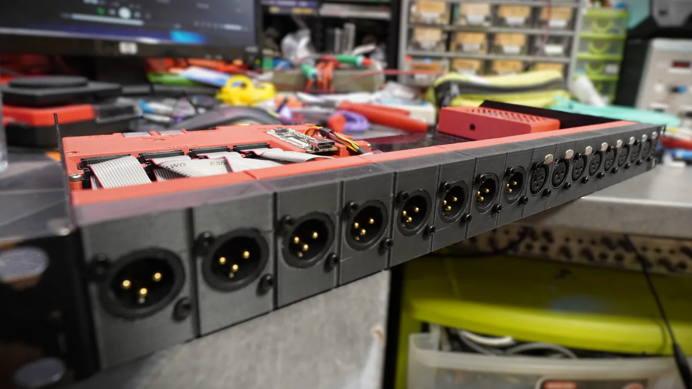
Designing the physical enclosure for this project turned out to be quite fun 😫. I didn't want to spend a bunch of money on a custom rack case, so instead I opted for the Scrooge McDuck 🦆 solution and used a standard 1U rack shelf. I've used this method in the past for my SDI over fiber project, so I knew it could work.
It's far from the best solution, but once everything is assembled, it's strong and, most importantly, very affordable. Using a shelf also means I don't have to worry about a custom front-panel or things like that. Instead I can just 3D-print the front and rear plates myself 👍.
Since the DAC and ADC modules have the same size, connector placement, and mounting holes, it was straightforward to design a holder for each. However, since this will be rack-mounted, I can't have screws on the bottom to attach the 3D prints. To solve this, I have 3 aluminum bars running for the whole length. These bars are then screwed in from the side:

I initially thought it wouldn't be enough and bought some strong double-sided tape. To my surprise, it turned out that it is surprisingly strong once all the holders are present 💪! My design made it so that 8 holders don't fill the full width, there's about a centimeter left that I use for status LEDs (like power, active, sync, …).
For the DAC/ADC holder, I designed a compact holder in which I can slide the PCB in from the rear and lock it against the faceplate with four M3 screws into the XLR connectors. Additionally, there are three M3 screws on the PCB itself; this increases the overall rigidity of the holder and makes sure it won't break when plugging in cables.


The only difference between the ADC and DAC holder is that the ADC one has an extra hole near each XLR connector for an LED, which will indicate the presence of phantom power 💡. Soldering the LEDs was quite annoying due to the short leads, so if anyone knows where I can get LEDs with longer leads, I would appreciate knowing about it!


I also designed some dust covers that you will see later. They slide in the dovetail-like slot of the sled. While it's by no means waterproof (or even dustproof), it will stop things from touching the PCB directly, which is the most important part for me.
The mainboard is going to get stuck on the shelf with double-sided tape, so I just needed a simple plate on the bottom to isolate the PCB from the metal shelf. And to make everything look good, I also made a front plate to cover most of the components:


I left the FPGA in the open because it's the only part on headers because I might use it for other projects in the future!
And it's finally time for assembly 🤩!
I started by putting the four DACs and four ADCs on their respective holders and sliding them into the shelf:


I then stuck the mainboard (and power supply) with some strong double-sided tape:


And finally I made "a few" custom cables to make sure everything looks neat:


Validation was quite fun because I discovered a few issues 😢:
These issues have been corrected in the schematics above
But after solving all of these, everything worked 🥳 !
Thanks to my dad, who's an actual sound engineer, and the Smaart software, I even managed to do some proper measurements 📏:

The signal is flat overall except in the lower frequencies. I suspect this is due to my choice of caps for the DAC 🤔, but it's more than good enough for me (in fact, it's better than what I measured at the output of the P16-M).
The software also gave me an estimate for latency, which is 0.56 ms (it's the equivalent of sitting ~20 cm from a speaker), which is again more than good enough for my application!
Ok enough text, let's see the demo 📹:
I didn't show every possible configuration but you can probably figure out how it would work. The last demo (with two boards) was filmed before the 2nd shelf arrived, hence why it doesn't look the same😅!
This project started with me wanting to carry timecode and a few other signals from stage to FOH and back. It then promptly spiraled out of control 🌪️ and fed my curiosity about the inner workings of Behringer's Ultranet and ended up as a robust, open hardware system I can actually trust on stage.
Just like my previous project, it taught me a lot. I learned about AES3 (and Ultranet) internals, clock domains ⌚, analog design, etc. This is huge because now when something goes wrong, I actually know what to look for, I can better estimate the limits of the systems I use, and I can figure out solutions to problems way faster. Working on a project like this not only gives you an insane amount of knowledge on the systems you are studying, but it also gives you a huge amount of respect for how much engineering goes into moving "just sixteen channels of audio".
Unlike the first part, I feel confident enough with my implementation to release this publicly on my GitHub. I do have to warn you that it's not a plug-and-play solution and requires a lot of work!
While it would be cool to look at XMOS chips, AES50, or even StageConnect now that it's open-source thanks to Chris, I don't think I'll touch audio stuff for a while now. However, I'm nowhere near done with live production tools. I've been playing with intercoms ☎️ (think ClearCom, RTS, …) for a few years now, and I've already invested quite a lot of time (and money) into making open-source analog and digital prototypes!
Want to chat about this article? Just post a message down here. Chat is powered by giscus and all discussions can be found here: TheStaticTurtle/blog-comments